01
Optical films
Measure optical response with phase and conductivity.
We test optical and photoelectrochemical film libraries to measure reflectance, absorption, transparency, conductivity, and phase before tests in the target layer stack.
Platform Characteristics
Deposition-to-characterization path.
02
Physical sample library
Create a real composition-spread thin-film library with 342 registered measurement positions.03
Composition map
Map element ratios by EDX/EDS or WDX for the material system.04
Structure and properties
Measure XRD phase data and selected electrical, mechanical, optical, magnetic, or electrochemical response.05
Scoped follow-up
Scanning droplet cell (SDC), SECCM, XPS, microscopy, or interface analysis can be added when surface change or a localized measurement decides the next step.06
Next experiment
Measured maps, Bayesian optimization, or Gaussian-process selection support repeat samples or a narrower campaign.Material decision
Where this applies.
Relevant areas
Relevant questions include transparent, reflective, absorptive, photonic, photoresponse, and photoelectrochemical thin-film systems.
Experimental plan
Map optical response across thin-film libraries, align spectra with composition and phase, then select samples for coating, layer-stack, or photoresponse tests.
Examples
- Transparent films
- Reflectance-tuned films
- Absorption-tuned films
- Photoelectrochemical films
Methods used
- UV-VIS spectroscopy
- four-point probe
- XRD mapping
- composition mapping
- composition-property visualization
Measurements
- reflectance
- absorption
- band gap
- transparency
- conductivity
- phase
- thickness
Outputs
- optical-property maps
- optical-electrical tradeoff regions
- selected films
- samples for layer stack tests
What comes back: Measured optical film samples for coating layer stack, photonic-device, or photoelectrochemical tests.
Figures
Optical and oxide-film figures.
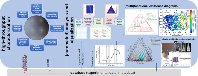
Library-scale characterization
Composition, structure, magnetic, electrical, optical, mechanical, and microstructure measurements feed measured maps.Ludwig, npj Comput. Mater. 2019, Fig. 2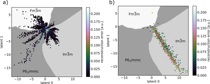
XRD dataset visualization
Library-scale diffraction data are grouped to compare phase behavior across measured thin-film samples.Banko et al., npj Comput. Mater. 2021, Fig. 2Closest Evidence
Closest optical and oxide-film demonstrations.
Piotrowiak et al., Adv. Eng. Mater. 2023
Perovskite oxide property ranges
Thin-film libraries were used to tailor optical band gap and electrical conductivity.Open sourcePiotrowiak et al., ACS Comb. Sci. 2020
Fe-Co-O optical mapping
Composition spreads connected phase, surface morphology, optical response, and electrode-layer stack behavior.Open sourcePlatform Basis
Methods behind the screen.
Ludwig, npj Comput. Mater. 2019
Combinatorial thin-film synthesis, high-throughput characterization, data handling, and composition-property mapping.Open sourceBanko et al., npj Comput. Mater. 2021
Deep-learning visualization and novelty detection for large XRD datasets from thin-film measurements.Open sourceReferences
Cited sources.
Ludwig, A. Discovery of new materials using combinatorial synthesis and high-throughput characterization of thin-film materials libraries combined with computational methods. npj Comput. Mater. 5, 70 (2019).
Combinatorial thin-film synthesis, high-throughput characterization, data handling, and composition-property mapping.
Piotrowiak, T. H.; Zehl, R.; Suhr, E.; Kohnen, B.; Banko, L.; Ludwig, A. Combinatorial Sputter Synthesis of Single-Phase La(XYZ)O3+-sigma Perovskite Thin-Film Libraries: A New Platform for Materials Discovery. Adv. Eng. Mater. 2023, 25 (16), 2300437.
Perovskite oxide thin-film libraries with phase, band-gap, conductivity, and catalyst-relevant screening.
Piotrowiak, T. H.; Wang, X.; Banko, L.; Kumari, S.; Sarker, S.; Mehta, A.; Ludwig, A. High-Throughput Characterization of (FexCo1-x)3O4 Thin-Film Composition Spreads. ACS Comb. Sci. 2020, 22 (12), 804-812.
Fe-Co-O composition spreads with phase, surface, optical, and electrode-stack-related characterization.
Banko, L.; Maffettone, P. M.; Naujoks, D.; Olds, D.; Ludwig, A. Deep learning for visualization and novelty detection in large X-ray diffraction datasets. npj Comput. Mater. 7, 104 (2021).
Deep-learning visualization and novelty detection for large XRD datasets from thin-film measurements.