01
Protective coatings
Screen conductive protective coatings and layer-stack candidates.
We test coating and interface libraries to map corrosion potential, contact resistance, mechanical response, and surface change before hardware or package-level tests.
Platform Characteristics
Deposition-to-characterization path.
02
Physical sample library
Create a real composition-spread thin-film library with 342 registered measurement positions.03
Composition map
Map element ratios by EDX/EDS or WDX for the material system.04
Structure and properties
Measure XRD phase data and selected electrical, mechanical, optical, magnetic, or electrochemical response.05
Scoped follow-up
Scanning droplet cell (SDC), SECCM, XPS, microscopy, or interface analysis can be added when surface change or a localized measurement decides the next step.06
Next experiment
Measured maps, Bayesian optimization, or Gaussian-process selection support repeat samples or a narrower campaign.Material decision
Where this applies.
Relevant areas
Relevant systems include conductive protective surfaces, bipolar-plate coating directions, adhesion layers, current collectors, bonding layers, and films or interfaces near layer-stack integration.
Experimental plan
Prepare coating or interface libraries, map composition and structure, measure corrosion potential with scanning droplet cell (SDC) and contact resistance with four-point probe, then select samples for reliability tests.
Examples
- Bipolar plate coating directions
- Conductive protective surfaces
- Adhesion and bonding layers
- Current-collector, bonding, and layer-stack films
Methods used
- co-sputtered alloy libraries
- reactive sputtering
- scanning droplet cell (SDC)
- four-point probe
- XRD mapping
- nanoindentation
Measurements
- composition
- phase
- corrosion potential
- contact resistance
- hardness or modulus
- surface change
Outputs
- coating composition or process ranges for follow-up
- corrosion-potential maps
- contact-resistance maps
- samples for coupon or package-level tests
What comes back: Measured coating and interface samples for hardware reliability, package-level reliability, or production qualification tests.
Figures
Coating and process figures.
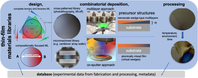
Combinatorial thin-film workflow
A material library connects synthesis, high-throughput characterization, data handling, and candidate selection.Ludwig, npj Comput. Mater. 2019, Fig. 1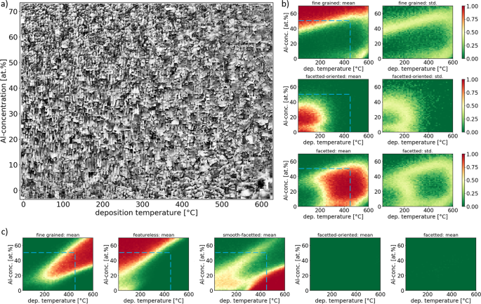
Structure-zone diagram
Measured and predicted microstructure classes define process ranges for thin-film samples.Banko et al., Commun. Mater. 2020, Fig. 6Closest Evidence
Closest coating and surface demonstrations.
Buenconsejo et al., ACS Comb. Sci. 2012
Twenty-four libraries for irreversible tests
Multiple ternary thin-film libraries were prepared on one substrate for tests such as etching, annealing, and exposure.Open sourceBanko et al., ACS Comb. Sci. 2019
Cr-Al-N coating process maps
Reactive sputtering, XRD, plasma diagnostics, hardness, and elastic modulus were connected for coating development.Open sourceRUB ELAN nanoelectrochemistry
Local electrochemical access
Scanning electrochemical methods support localized electrochemical measurements on defined regions.Open sourcePlatform Basis
Methods behind the screen.
Ludwig, npj Comput. Mater. 2019
Combinatorial thin-film synthesis, high-throughput characterization, data handling, and composition-property mapping.Open sourceBanko et al., Commun. Mater. 2020
Processing libraries and generative machine learning used to select thin-film microstructure ranges.Open sourceReferences
Cited sources.
Ludwig, A. Discovery of new materials using combinatorial synthesis and high-throughput characterization of thin-film materials libraries combined with computational methods. npj Comput. Mater. 5, 70 (2019).
Combinatorial thin-film synthesis, high-throughput characterization, data handling, and composition-property mapping.
Buenconsejo, P. J. S.; Siegel, A.; Savan, A.; Thienhaus, S.; Ludwig, A. Preparation of 24 Ternary Thin Film Materials Libraries on a Single Substrate in One Experiment for Irreversible High-Throughput Studies. ACS Comb. Sci. 2012, 14 (1), 25-30.
Twenty-four ternary thin-film libraries on one substrate for irreversible tests.
Banko, L.; Ries, S.; Grochla, D.; Arghavani, M.; Salomon, S.; Pfetzing-Micklich, J.; Kostka, A.; Rogalla, D.; Schulze, J.; Awakowicz, P.; Ludwig, A. Effects of the Ion to Growth Flux Ratio on the Constitution and Mechanical Properties of Cr1-x-Alx-N Thin Films. ACS Comb. Sci. 2019, 21 (12), 782-793.
Reactive DC magnetron sputtering, automated XRD, plasma diagnostics, hardness, and elastic modulus for Cr-Al-N films.
Banko, L.; Lysogorskiy, Y.; Grochla, D.; Naujoks, D.; Drautz, R.; Ludwig, A. Predicting structure zone diagrams for thin film synthesis by generative machine learning. Commun. Mater. 1, 15 (2020).
Processing libraries and generative machine learning used to select thin-film microstructure ranges.
RUB ELAN nanoelectrochemistry
Scanning electrochemical methods for local measurements on defined material regions.